S-100 system you will need a "Prototype Board". This is a
card that fits into your S-100 bus and brings the bus edge connector pins (all
100 of them) up on to the board. Almost from the very start
companies supplied these boards for what was at the time a hobbyists market.
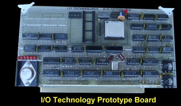
Here is a picture of a typical board:-
Typically you laid out the chips horizontally (although some vertical
orientation boards were produced). These board can be found on
places like eBay from time to time. When later non-DIP style
chips (CPU's etc.) started to appear these boards did not work. One or two
companies offered boards with just 0.1" pad spacing or a board with at least
an area with this format such as this
I/O Technology
board.
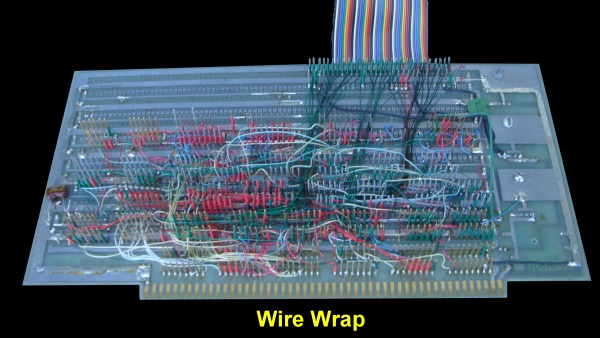
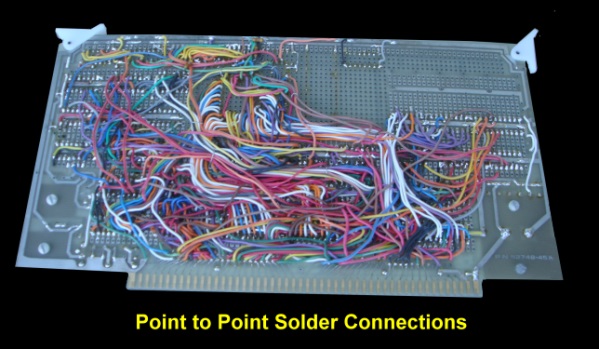
Connecting the IC pins together can be done either via wire wrap or
point to point solder techniques. There are pros and cons to
each method. Here are two examples:-
Personally I prefer the point to point soldering
method. It takes longer to do initially but in the end you save time
debugging because it is easier to locate connections and make changes.
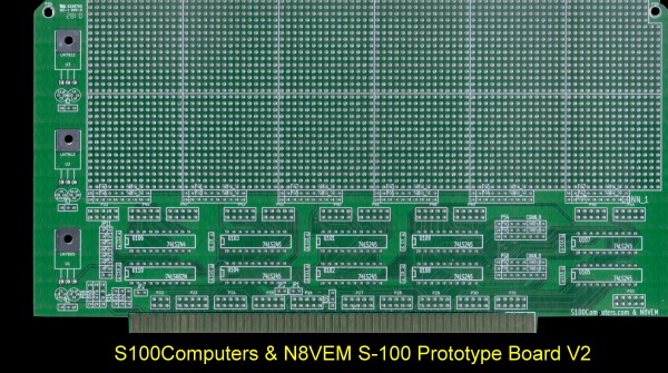
A Buffered S-100 Prototype Board
One of the frustrating aspects of doing a new prototype board design is that
before you can do anything useful you have to connect up all the address
lines (24) , data lines (16) and numerous control line to buffers on the
board. Each requires an input line from the bus and an output line to
the functional area of the board. For almost every board they will be the
same. To take the drudgery out of this I have designed with Andrew at
N8VEM a "buffered prototype S-100" board with all these connections already
done. Here is a picture of the board:-
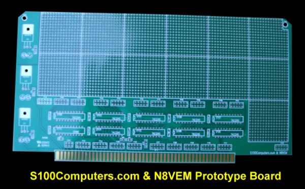
There are distinct pads for all the major buffered S-100 lines. You can
start right away utilizing the board for what you had in mind. The
schematic for the board is quite simple and can be seen
here.
The layout for the board can be seen
here. There are pads for a +5V, +12V and -5V or -12V voltage
regulator. The only slightly unusual thing is U108, a 74LS245 buffer
that may be used to transfer data to/from the 8 bit data In/Out lines. This
can sometimes be of use for interrupts in 16 bit systems. Unfortunately its
on the S-100 side of bus buffers and so cannot be used for 16 bit CPU data
transfers if you wanted to use this board as an 16 Bit CPU prototype board.
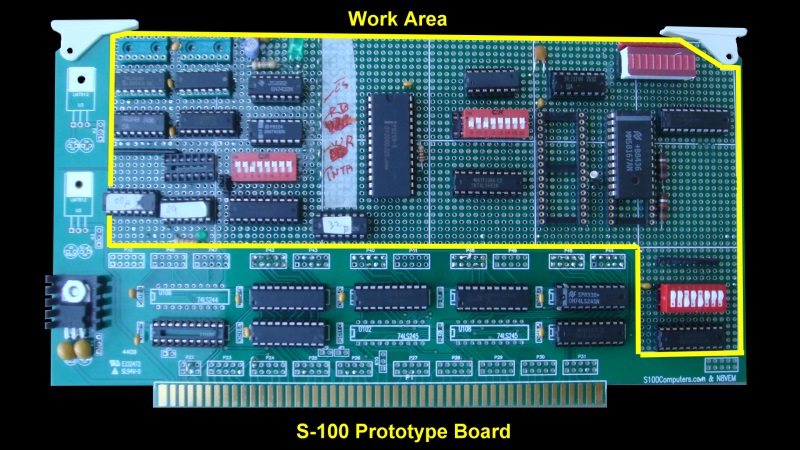
I have use this board for a number of S-100 prototype boards. Here is
a picture of it being used for the first
PIC/RTC board:-
V2 of the Buffered S-100 Prototype
Board.
Having utilized a number of these boards, I realized that a few little
tweaks would make a big difference. So with Andrews's help we designed a
second version of the board. This board has in addition to the board
above:-
1. I/O port selection
circuitry that can be jumpered for any 8 bit I/O address range.
2. A complete bi-directional buffer (U108) setup for
8/16 bit data transfers with 16 bit CPU's.
3. A dedicated 5V line across the bottom of the "patch"
area for convenient hookup to IC's.
4. Complete flexibility as to the type or Voltage
regulators used in each of the 3 positions.
The schematic for the V2 Prototype board can be obtained
here. The board layout can be obtained
here.
The board utilizes
74LS682's for port addressing. If your are unfamiliar with this technique
click
here.
A Production S-100 Board.
Realizing that a number of people might want to utilize a board like this
together
with Andrew Lynch at N8VEM (see
here) we have
completed a run of these boards. We will collect names for a second
batch if needed. If
you have an interest in such a bare board, let Andrew know via e-mail at:-
lynchaj@yahoo.com.
They will be about $20-$40 each (depending on demand) . As always, you get
your own parts, no hand holding or manual!